Beyond the Die: Why Advanced Packaging Became the Real AI Silicon Bottleneck
Why CoWoS packaging and advanced packaging capacity—not just wafer fabs—now limit AI accelerators, and how TSMC, ASE and SPIL are racing to expand.
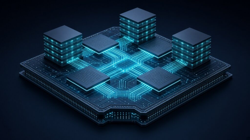
For most of the semiconductor era, “capacity” meant wafer starts. In the AI boom, a finished accelerator only exists after advanced packaging joins compute dies to high-bandwidth memory. That back-end step—CoWoS packaging and its rivals—has become the scarce resource that decides how many AI chips the world can ship.
The bottleneck moved downstream
Front-end foundries still matter. TSMC’s third-quarter 2026 results show how tightly AI demand is tied to leading-edge silicon: revenue reached USD 46.72 billion, high-performance computing contributed 68% of revenue, and technologies at 7 nm and below accounted for 79% of wafer revenue [1][2]. On the October 15, 2026 earnings call, Chairman and CEO C.C. Wei said AI-related demand remains “extremely robust,” that TSMC is building 13 leading-edge and advanced packaging fabs in Taiwan over the next several years plus five to six fabs overseas, and that the company has “no intention to leave food on the table” [1].
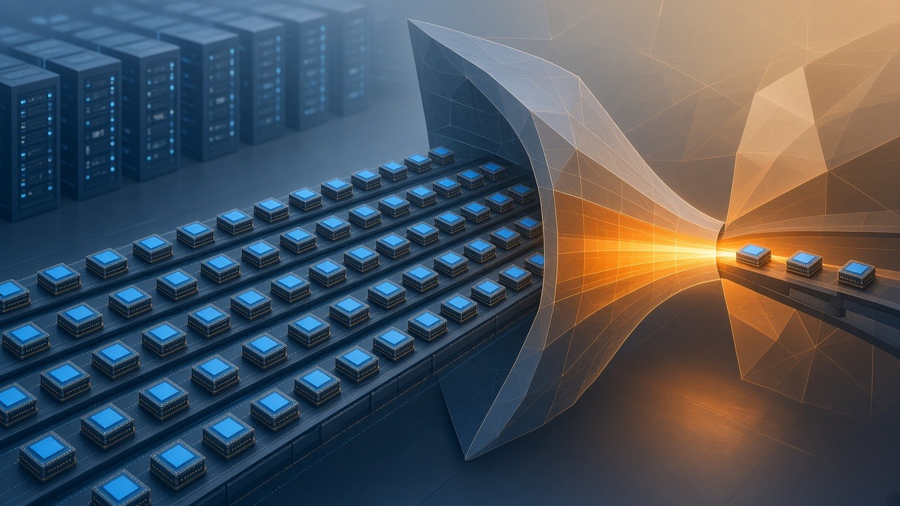
Yet Wei’s own Q&A answers show where the constraint has shifted. Asked about larger reticle packages and competitors such as Intel’s EMIB-T, he said TSMC is already in real production of 5x reticle-size advanced packaging with “excellent” yield, is working on 9x and moving toward 14x, and is developing CoPoS for future cost reduction—while insisting that “so far, the CoWoS is still the number one choice for our customers” [1]. He also signaled that helping customers introduce products smoothly is TSMC’s first priority if a rival packaging path falls short [1].
In plain language: a 2 nm or 3 nm die is not yet an AI accelerator. It becomes one only after it is bonded to high-bandwidth memory on a large interposer or similar construct. That is what advanced packaging means for AI chips in practice, and CoWoS is still the industry’s default path for the densest parts.
What CoWoS actually does
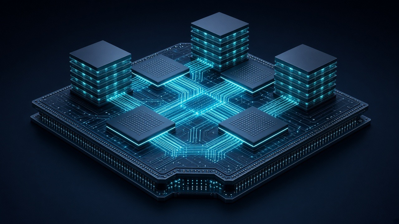
Chip-on-Wafer-on-Substrate (CoWoS) is TSMC’s flagship 2.5D advanced packaging platform. It places one or more logic dies and multiple HBM stacks on a silicon interposer so they behave as a single, high-bandwidth system. As packages grow—more compute dies, more HBM cubes, larger reticle multiples—each finished unit consumes more packaging resources. Doubling packaging wafer capacity does not automatically double the number of finished accelerators if each package is getting bigger.
That math is why packaging lead times and pricing have become board-level topics. TrendForce, citing Commercial Times and supply-chain sources, reported on October 27, 2026 that foundries and OSAT providers were considering another round of CoWoS price increases of about 10%–20%, that some packaging lead times were stretching, and that equipment lead times had lengthened to roughly six to eight months [3]. Those figures are TrendForce’s report of supply-chain commentary—not confirmed TSMC guidance—and should be read that way. Separately, TrendForce noted analyst estimates that monthly CoWoS capacity could exceed roughly 130,000 wafers in 2026 and rise further in 2027, alongside TSMC’s public comments on 5x reticle production and CoPoS development [3].
The commercial pressure shows up in press reporting as well. In a November 6, 2026 Reuters investigation from Taipei, reporters wrote that AI demand has turned advanced packaging into a “critical bottleneck,” that revenue from advanced packaging is forecast by Yole Group to overtake traditional packaging for the first time in 2026, and that capital spending on the technology is expected to near USD 28 billion [4]. Reuters also reported, citing an industry executive familiar with the matter, that Nvidia is providing billions of dollars in financing to expand CoWoS packaging capacity at Siliconware Precision Industries (SPIL), a unit of ASE Technology; Nvidia did not comment, and ASE said it does not comment on market rumours involving customers [4].
TSMC’s official stance: expand, enlarge packages, keep CoWoS first
TSMC’s investor materials put numbers around the AI pull. For the third quarter of 2026 the company reported USD 46.72 billion in revenue, a 66.4% gross margin and a 58.7% operating margin, and guided fourth-quarter revenue to USD 52.3–54.3 billion [2]. CFO Wendell Huang reiterated a 2026 capital budget of USD 60–64 billion and said CapEx from 2026 to 2028 is expected to be “significantly higher” than the prior three years [1]. Wei raised full-year 2026 revenue growth guidance to around 44% year over year in U.S. dollar terms and said previously guided AI-accelerator CAGR in the mid- to high-50% range from 2024 to 2029 “probably will be higher” [1].
On packaging specifically, the earnings call is the primary source. Wei’s points worth retaining:
- CoWoS remains customers’ number-one packaging choice today [1].
- 5x reticle-size packaging is in volume production with excellent yield; 9x is in development and 14x is on the roadmap [1].
- CoPoS is in development to enable future cost reduction for larger packages [1].
- TSMC will prioritize getting customers’ products to market if a competitor’s packaging solution cannot meet demand [1].
- TSMC has also partnered on back-end supply, including a deal with GlobalFoundries on interposers, because back-end capacity is tight [1].
None of that is a monthly CoWoS capacity figure from TSMC itself. Analyst wafer estimates circulating in trade press remain secondary. What is primary is TSMC’s insistence that its CoWoS capacity—and the larger packages riding on it—is central to capturing AI demand.
OSATs move in: ASE’s panel bet and SPIL’s AI plants
When a foundry’s packaging lines are full, outsourced assembly and test (OSAT) vendors become strategic. ASE Technology Holding’s assembly arm has made that explicit. In a May 26, 2026 press release, Advanced Semiconductor Engineering (ASE) announced what it called an industry-first automated 310 mm × 310 mm panel-level packaging production line, expected to enter production in the first half of 2027 [5]. ASE said the rectangular panel format offers up to 96,100 mm² of usable area versus round wafers, supports FOCoS and FOCoS-Bridge platforms, and targets AI and HPC packages that keep growing in size and I/O density [5]. Executive Vice President Yin Chang framed panel-level packaging as necessary because “achieving the highest levels of system performance requires not only advanced silicon, but also advances in packaging efficiency and integration” [5].
SPIL, ASE’s wholly owned subsidiary, has been expanding advanced assembly capacity for AI processors in central Taiwan. In an ASE Holdings press release dated January 16, 2025, SPIL said Nvidia founder and CEO Jensen Huang attended the opening of its Tan Ke Plant, that the site is designed for Nvidia accelerated computing and had reached ramp-up, and that SPIL was expanding plants in Changhua, Erlin and Huwei (Yunlin), with planning underway for a new factory site in Douliu, Yunlin [6].
Taiwan’s Central News Agency, via Focus Taiwan, later reported that on August 12, 2026 SPIL broke ground on a NT$100 billion (about USD 3.11 billion) CoWoS packaging and testing plant in Douliu, Yunlin, with first-phase operations scheduled for 2028 and about 2,200 jobs planned when fully online [7]. Focus Taiwan attributed those details to remarks by SPIL Vice Chairman Chang Yen-chun at the groundbreaking and noted SPIL’s board approval of a rights issue to fund materials and capacity, with ASE set to subscribe [7]. That is press reporting of a company event—not an ASE/SPIL web press release—and is cited here as such.
Reuters’ November 2026 package also described how designers are seeking capacity outside TSMC: Powertech Technology’s chairman said customers “don’t want to rely entirely on TSMC,” and Powertech is investing about USD 400 million in a panel-level packaging joint venture with Broadcom in Singapore with production eyed for 2028 [4]. AMD CEO Lisa Su told Reuters in Taipei in October that CoWoS and advanced packaging are “super important” for high-performance computing and that “we do need more capacity overall” [4].
Why packaging scarcity reshapes AI power players
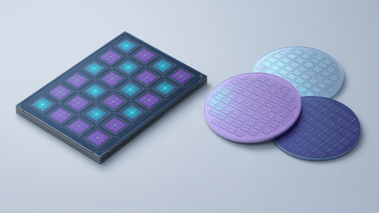
Advanced packaging changes competitive dynamics in three ways.
First, it reallocates scarcity. When CoWoS slots are short, the constraint is not only which foundry can print the logic die, but which back-end line can finish the module. Hyperscalers and GPU vendors that secure packaging allocations can ship; those that cannot wait. That is why financing packaging capacity—which Reuters, citing an unnamed industry executive, reported Nvidia is doing at SPIL—belongs in the same strategic conversation as buying wafers [4].
Second, it pulls OSATs into the AI power-players tier. ASE’s panel-level roadmap and SPIL’s AI-focused plants are no longer “backend commodity” stories. They are capacity plays that determine how many Blackwell-, Rubin-, Instinct- or custom-ASIC-class parts leave the factory. TSMC still leads high-end packaging, but its own call acknowledged back-end shortage and partnering for interposers [1].
Third, package size fights capacity math. Wei’s 5x-to-14x reticle roadmap means each next-generation accelerator may consume more packaging area per unit [1]. ASE’s panel pitch is an attempt to raise usable area per manufacturing run [5]. Both responses admit the same problem: wafer-equivalent packaging capacity can rise while unit shipments of finished AI accelerators rise more slowly.
For operators building AI hyperscale infrastructure, the planning implication is direct. Lead times now include packaging and final test, not only wafer fab queues. Bill-of-materials cost increasingly embeds advanced packaging value—Reuters quoted former Intel CEO Pat Gelsinger estimating packaging could eventually account for as much as half the value of a chip product as designs integrate 10 or more chips [4]. And geographic concentration matters: most leading CoWoS-class capacity still sits in Taiwan, even as TSMC and OSATs discuss overseas packaging footprints [1][4].
What to watch next
Three primary signals will show whether the packaging bottleneck eases:
- TSMC’s next earnings commentary on CoWoS, CoPoS and reticle-size progress—especially whether 9x moves from development into production [1].
- ASE’s 310 mm panel line entering production in the first half of 2027 and winning real AI package qualifications [5].
- SPIL’s Douliu CoWoS ramp toward 2028 first-phase operations, as reported at the August 2026 groundbreaking [7].
Until those lines add finished modules at scale, advanced packaging—not the lithography scanner alone—remains the binding constraint on how fast the AI silicon supply chain can grow.
Related reading
- The HBM4 Supply Race: Samsung, SK hynix, and Micron Rewrite AI Memory Economics
- Multi-Trillion-Parameter Training: What the Next Silicon Generation Must Deliver
- The AI Accelerator Market: GPUs, ASICs and the Second-Source Race
- Equity for Silicon: How AMD Turned OpenAI and Meta Into Stakeholders
References / Sources
- Taiwan Semiconductor Manufacturing Company, Q3 2026 Earnings Conference Call Transcript (Oct. 15, 2026): https://investor.tsmc.com/english/encrypt/files/encrypt_file/reports/2026-10/eba4fac72873bf546b669bd2b5d973df5c93215d/TSMC%203Q26%20Transcript.pdf
- TSMC, Financial Results — 2026Q3: https://investor.tsmc.com/english/quarterly-results/2026/q3
- TrendForce, “TSMC Reportedly Eyes 20% CoWoS Price Hike…” (Oct. 27, 2026) — supply-chain report, not TSMC confirmation: https://www.trendforce.com/news/2026/10/27/news-tsmc-reportedly-eyes-20-cowos-price-hike-skips-equipment-price-renegotiations-amid-ai-demand-surge/
- Reuters, Wen-Yee Lee, “AI boom turns chip packaging into the next battleground for semiconductors” (Nov. 6, 2026): https://www.reuters.com/5f374b32b07b/world/asia-pacific/ai-boom-turns-chip-packaging-into-next-battleground-semiconductors-2026-11-06/
- ASE Holdings press release, “ASE Launches Automated 310mm Panel-Level Packaging to Accelerate AI Innovation” (May 26, 2026): https://www.aseglobal.com/press-room/310×310/
- ASE Holdings press release, “SPIL hosts NVIDIA founder and CEO Jensen Huang at new factory site…” (Jan. 16, 2025): https://www.aseglobal.com/press-room/spil-hosts-nvidia-founder-and-ceo-at-new-factory-site
- Focus Taiwan / CNA, “SPIL breaks ground on advanced IC packaging, testing plant in Yunlin” (Aug. 12, 2026) — press report of SPIL groundbreaking remarks: https://focustaiwan.tw/business/202608120005
Images: original illustrations generated for AndBeyond.Tech; no logos or real people depicted.