Multi-Trillion-Parameter Training: What the Next Silicon Generation Must Deliver
What next-gen AI training silicon must deliver for multi-trillion-parameter models: HBM, NVL72 scale-up, scale-out fabrics, liquid cooling and reliability.
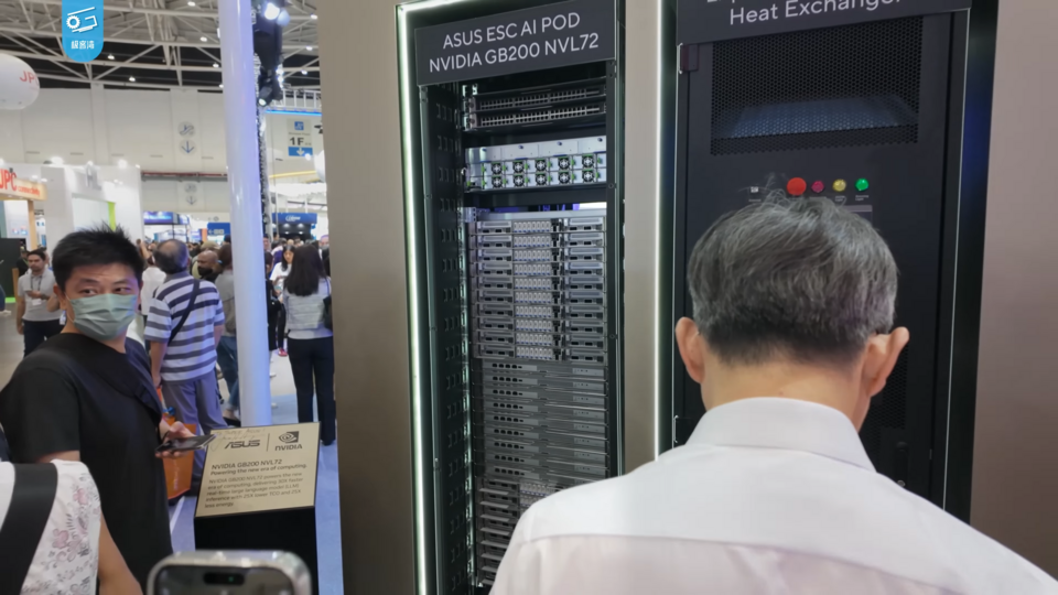
The compute ceiling for frontier models is no longer set by any one chip. It is set by the whole system: how much high-bandwidth memory sits next to each processor, how many processors can share that memory over a fast scale-up fabric, how far the cluster scales out beyond the rack, and whether the building can power and cool it. This evergreen guide walks through those four constraints and looks at what NVL-class racks such as the GB200 NVL72 show about the next generation of AI training silicon.
Why “the chip” is the wrong unit of analysis
The clearest public look at what frontier-scale training really demands is still Meta’s paper on Llama 3. Meta trained its 405-billion-parameter model on “up to 16K H100 GPUs, each running at 700W TDP with 80GB HBM3.” Each server held eight GPUs connected via NVLink [1]. That model is a fraction of the multi-trillion-parameter scale the industry is now designing for, yet the paper describes problems at every layer of the system. They include memory capacity, network topology, failures, and power swings big enough to strain the grid. Those problems are a useful checklist for what next-generation hardware has to solve.
Meta is explicit that the model has to be split up just to fit. It used “4D parallelism,” combining tensor, pipeline, context and data parallelism. The aim was to ensure “each GPU’s model parameters, optimizer states, gradients, and activations fit in its HBM” [1]. Even with careful tuning, Meta reported a BF16 Model FLOPs Utilization (MFU) of 38–43% across its main configurations [1]. A large share of peak compute goes unused because of memory and communication overhead. Those two constraints are where the next silicon generation has to deliver.
Requirement 1: More HBM, and much more bandwidth to it
High-bandwidth memory (HBM) is the stacked DRAM placed right next to the accelerator die. For an HBM GPU, capacity decides how much of the model and its training state can live on each device. Bandwidth decides how quickly that data reaches the compute units.
The industry standard is moving quickly. JEDEC published the JESD270-4 HBM4 standard in April 2025. It specifies “transfer speeds up to 8 Gb/s across a 2048-bit interface,” which raises “total bandwidth up to 2 TB/s” per stack. It doubles independent channels per stack from 16 to 32, and supports stacks up to 16-high with “a higher cube density of 64GB” [2]. Among the industry statements in the release, Google Cloud’s quote says HBM4 “represents the big step in bandwidth that Google needs for next generation training and inference systems” [2].
The figures from shipping and announced accelerators show the trend:
- NVIDIA GB200 NVL72 (Blackwell, HBM3E): 13.4 TB of HBM3E per rack with 576 TB/s of aggregate bandwidth, or 372 GB and 16 TB/s per two-GPU Grace Blackwell Superchip [3].
- NVIDIA Vera Rubin NVL72 (HBM4): 288 GB of HBM4 at 19.2 TB/s per Rubin GPU, and 20.7 TB at 1,400 TB/s per rack, according to NVIDIA’s current product page [4].
- Google TPU7x (Ironwood): 192 GiB of HBM per chip at 7,380 GBps, against 95 GiB for v5p and 32 GiB for v6e (Trillium) [5].
Google’s documentation adds a caution that applies to every vendor: “despite its size, HBM can still be a bottleneck, particularly for memory-bound vector operations or inefficient data access patterns” [5]. More capacity lets a training job use larger batches and fewer shards. Bandwidth determines whether the compute units actually stay busy.
Published specs can also change. NVIDIA’s own pages are labeled “preliminary specifications; may be subject to change” [6]. Buyers planning a multi-trillion-parameter run should treat memory bandwidth figures as targets until they are measured on delivered systems.
Requirement 2: A bigger, faster scale-up domain
A model too large for one device must exchange activations and gradients constantly. The most bandwidth-hungry traffic, tensor parallelism and the all-to-all exchanges of mixture-of-experts (MoE) models, has to stay inside a scale-up domain. That is a group of accelerators linked by a memory-semantic fabric far faster than a regular network.
Meta’s Llama 3 paper explains why. Parallelism dimensions were ordered so that “the innermost parallelism requires the highest network bandwidth and lowest latency, and hence is usually constrained to within the same server” [1]. In Meta’s cluster, that meant eight GPUs.
The NVL-class rack exists to make that boundary much larger. NVIDIA describes the GB200 NVL72 as connecting “36 Grace CPUs and 72 Blackwell GPUs in a rack-scale, liquid-cooled design” with “a 72-GPU NVIDIA NVLink domain that acts as a single, massive GPU.” Its NVLink Switch System provides “130 terabytes per second (TB/s) of low-latency GPU communications,” with fifth-generation NVLink giving each GPU 1.8 TB/s [3]. NVIDIA’s NVLink specification table traces the progression across generations:
| NVLink generation | Platform | Bandwidth per GPU | NVLink domain | Aggregate (NVL72) |
|---|---|---|---|---|
| 4th | Hopper | 900 GB/s | 8 GPUs | 7.2 TB/s (8-GPU) |
| 5th | Blackwell | 1,800 GB/s | 8 or 72 GPUs | 130 TB/s |
| 6th | Vera Rubin | 3,000 GB/s | 8 or 72 GPUs | 216 TB/s |
Source: NVIDIA NVLink specifications page (preliminary) [6].
According to NVIDIA, an NVL72 rack “can support 9x the GPU count versus a single eight-GPU system” within one NVLink domain [6]. For the Vera Rubin generation, NVIDIA claims the NVL72 “trains mixture-of-experts (MoE) models with one-fourth the number of GPUs compared to NVIDIA GB200 NVL72.” That is a projection based on “a 10T MoE model trained on 100T tokens in a fixed timeframe of 1 month” [4]. The benchmark scenario NVIDIA chose is itself a ten-trillion-parameter model, which shows the scale the industry now designs for.
NVLink is not the only approach. Google’s TPU7x links each chip directly to its neighbors in a 3D torus. Slices are built from 4×4×4 “cubes,” and a pod scales to 9,216 chips (144 cubes), with 1,200 GBps of total bidirectional inter-chip interconnect bandwidth per chip [5]. Open standards are also arriving. The UALink Consortium ratified its UALink 200G 1.0 Specification in April 2025. It enables “200G per lane scale-up connection for up to 1,024 accelerators within an AI computing pod,” with a board that includes AMD, AWS, Google, Intel, Meta and Microsoft [7]. Whichever fabric wins, the requirement is the same: larger coherent domains with predictable latency.
Requirement 3: Scale-out networks that don’t waste the scale-up gains
No rack is big enough on its own for a frontier run, so NVL72 AI cluster designs still depend on scale-out networking between racks. Here, too, Meta’s paper is unusually specific. Its RoCE cluster for Llama 3 was a three-layer Clos network. Pods of 3,072 GPUs had full bisection bandwidth, but the aggregation layer connecting eight pods into a 24K-GPU cluster had “an oversubscription ratio of 1:7.” Meta made its parallelism and scheduler “network topology” aware to minimize traffic across pods [1]. Meta also had to work around load-balancing problems because LLM training “produces fat network flows that are hard to load balance” [1].
Vendors are building more bandwidth and smarter transport into the scale-out tier. NVIDIA lists 32.4 TB/s of networking bandwidth per Vera Rubin NVL72 rack, with scale-out over Quantum-X800 InfiniBand or Spectrum-X Ethernet [4]. On the open side, the Ultra Ethernet Consortium released UEC Specification 1.0 in June 2025. It describes the spec as “a comprehensive, Ethernet-based communication stack engineered to meet the demanding needs of modern Artificial Intelligence (AI) and High-Performance Computing (HPC) workloads,” covering “NICs, switches, optics, and cables,” and says it “scales to millions of endpoints” [8].
The design principle follows from the Llama 3 experience. Put the most communication-intensive parallelism inside the scale-up domain, and make the scale-out fabric good enough that data-parallel and pipeline traffic does not stall the job.
Requirement 4: Power density and liquid cooling
Packing 72 GPUs into a single NVLink domain means packing them into one rack, and that changes the facility. Vertiv’s reference architecture co-developed with NVIDIA for the GB200 NVL72 “supports up to 132kW per rack.” It uses a hybrid liquid- and air-cooling design to “efficiently manage high-density heat removal,” and scales to a 7MW deployment [9]. NVIDIA’s own pages describe the NVL72 as liquid-cooled. They say liquid cooling “increases compute density, reduces the amount of floor space used, and facilitates high-bandwidth, low-latency GPU communication with large NVLink domain architectures” [3]. For Vera Rubin NVL72, NVIDIA lists a 45°C coolant inlet temperature [4].
NVIDIA’s own wording ties the two together: the dense, liquid-cooled rack is what makes the large NVLink domain practical [3]. The scale-up requirement and the cooling requirement are the same problem seen from two sides.
Power is not only a question of density. It is also about how quickly the load swings. Meta reported that during training, “tens of thousands of GPUs may increase or decrease power consumption at the same time,” for example while waiting on checkpoints or collective operations. This “can result in instant fluctuations of power consumption across the data center on the order of tens of megawatts, stretching the limits of the power grid” [1]. Meta also observed “a diurnal 1-2% throughput variation” linked to mid-day temperatures affecting GPU voltage and frequency scaling [1]. Vertiv’s architecture includes “load averaging via lithium-ion battery and next generation UPS” to “support dynamic GPU workloads” [9]. Infrastructure is starting to respond to this problem directly.
Requirement 5: Reliability at scale
The bigger the synchronous job, the more costly every fault becomes. Meta wrote that “a single GPU failure may require a restart of the entire job.” Over a 54-day snapshot of Llama 3 pre-training it recorded 466 job interruptions, 419 of them unexpected. About 78% of the unexpected ones were attributed to confirmed or suspected hardware issues [1]. Faulty GPUs (148 interruptions, 30.1%) and GPU HBM3 memory (72, 17.2%) were the two largest categories [1]. Meta still achieved “higher than 90% effective training time” through automation, faster checkpointing and diagnostic tooling [1].
For multi-trillion-parameter training on far more devices, serviceability is a silicon and system requirement in its own right. NVIDIA’s NVLink 6 Switch adds “control plane resilience, the ability to run with a partially populated rack, and hot-swapping of switch trays” [6]. JEDEC’s HBM4 standard includes Directed Refresh Management “for improved row-hammer mitigation and Reliability, Availability, and Serviceability (RAS)” [2]. These features get less attention than FLOPS, but at cluster scale they can decide whether a training run finishes on schedule.
The checklist: what next-generation AI training silicon must deliver
Combining the evidence above, a credible platform for multi-trillion-parameter training needs to deliver:
- HBM capacity and bandwidth that grow faster than compute. HBM4-class stacks [2] and per-device capacity in the hundreds of gigabytes [4][5], so parameters, optimizer states and activations can be sharded across fewer devices [1].
- A large scale-up domain. Dozens of devices or more with all-to-all bandwidth measured in terabytes per second per device [3][6], or open alternatives such as UALink that target up to 1,024 accelerators [7].
- A topology-aware scale-out fabric. One that limits the cost of oversubscription [1], built on InfiniBand or AI-tuned Ethernet [4][8].
- Rack power and cooling designed together with the silicon. Liquid-cooled racks in the 100+ kW class [9], with power smoothing for synchronous load swings [1][9].
- Reliability features built in. Memory RAS [2], resilient switch fabrics [6], and software that recovers automatically [1].
Bottom line
The race to train multi-trillion-parameter models is a race to build balanced systems. The industry’s own data shows that memory capacity, interconnect bandwidth, facility power and failure handling can each become the limiting factor before raw FLOPS does. NVL72-class racks, HBM4 and open scale-up and scale-out standards are the industry’s current answers. When judging the next AI training silicon launch, look past the headline FLOPS. Check the memory, the size of the scale-up domain, the watts per rack, and how gracefully the system copes when a part fails.
Related reading
- Inside the AI Accelerator Market: GPUs, Custom ASICs, and Who Wins Inference
- InfiniBand vs Ethernet for AI Clusters: The Fabric War Inside the AI Factory
- How Distributed AI Superfactories Stretch the Network Between Campuses
References / Sources
- Llama Team, AI @ Meta — “The Llama 3 Herd of Models” (arXiv:2407.21783, July 2024), §3.3. https://arxiv.org/html/2407.21783v2
- JEDEC — “JEDEC and Industry Leaders Collaborate to Release JESD270-4 HBM4 Standard” (Apr 16, 2025). https://www.jedec.org/news/pressreleases/jedec%C2%AE-and-industry-leaders-collaborate-release-jesd270-4-hbm4-standard-advancing
- NVIDIA — “GB200 NVL72” product page. https://www.nvidia.com/en-us/data-center/gb200-nvl72/
- NVIDIA — “Vera Rubin NVL72” product page. https://www.nvidia.com/en-us/data-center/vera-rubin-nvl72/
- Google Cloud Documentation — “TPU7x (Ironwood)” (last updated Oct 29, 2026). https://docs.cloud.google.com/tpu/docs/tpu7x
- NVIDIA — “NVLink and NVLink Switch” (specifications, preliminary). https://www.nvidia.com/en-us/data-center/nvlink/
- UALink Consortium — “UALink Consortium Releases the Ultra Accelerator Link 200G 1.0 Specification” (Apr 8, 2025). https://ualinkconsortium.org/wp-content/uploads/2025/04/UALink-1.0-Specification-PR_FINAL.pdf
- Ultra Ethernet Consortium — “UEC Launches Specification 1.0” (Jun 11, 2025). https://ultraethernet.org/ultra-ethernet-consortium-uec-launches-specification-1-0-transforming-ethernet-for-ai-and-hpc-at-scale/
- Vertiv — “Vertiv codevelops with NVIDIA complete power and cooling blueprint for NVIDIA GB200 NVL72 platform” (Oct 15, 2024). https://prod.vertiv.cn/en-asia/about/news-and-events/news-releases/vertiv-codevelops-with-nvidia-complete-power-and-cooling-blueprint-for–nvidia-gb200-nvl72-platform/
Images: illustrations generated for AndBeyond.Tech, except: NVIDIA GB200 NVL72 rack on display — 极客湾Geekerwan, Wikimedia Commons, CC BY 3.0; HBM cross-section diagram — 思考的苇丛, Wikimedia Commons, CC BY-SA 4.0.